- 您现在的位置:买卖IC网 > Sheet目录362800 > EVAL-AD5532EB (Analog Devices, Inc.) 32-Channel, 14-Bit Voltage-Output DAC
REV. 0
AD5532
TIMING CHARACTERISTICS
PARALLEL INTERFACE
–4–
Limit at T
MIN
, T
MAX
(A Version)
Parameter
1, 2
Unit
Conditions/Comments
t
1
t
2
t
3
t
4
t
5
t
6
0
0
50
50
20
0
ns min
ns min
ns min
ns min
ns min
ns min
CS
to
WR
Setup Time
CS
to
WR
Hold Time
CS
Pulsewidth Low
WR
Pulsewidth Low
A4–A0, CAL, OFFS_SEL to
WR
Setup Time
A4–A0, CAL, OFFS_SEL to
WR
Hold Time
NOTES
1
See Interface Timing Diagram.
2
Guaranteed by design and characterization, not production tested.
Specifications subject to change without notice.
SERIAL INTERFACE
Limit at T
MIN
, T
MAX
(A Version)
Parameter
1, 2
f
CLKIN3
t
1
t
2
t
3
t
4
t
5
t
6
t
7
t
84
t
94
t
10
t
11
Unit
Conditions/Comments
14
28
28
10
50
10
5
5
20
60
400
400
MHz max
ns min
ns min
ns min
ns min
ns min
ns min
ns min
ns max
ns max
ns min
ns min
SCLK Frequency
SCLK High Pulsewidth
SCLK Low Pulsewidth
SYNC
Falling Edge to SCLK Falling Edge Setup Time
SYNC
Low Time
D
IN
Setup Time
D
IN
Hold Time
SYNC
Falling Edge to SCLK Rising Edge Setup Time
SCLK Rising Edge to D
OUT
Valid
SCLK Falling Edge to D
OUT
High Impedance
10th SCLK Falling Edge to
SYNC
Falling Edge for Readback
24th SCLK Falling Edge to
SYNC
Falling Edge for DAC Mode Write
NOTES
1
See Serial Interface Timing Diagrams.
2
Guaranteed by design and characterization, not production tested.
3
In SHA mode the maximum SCLK frequency is 20 MHz and the minimum pulsewidth is 20 ns.
4
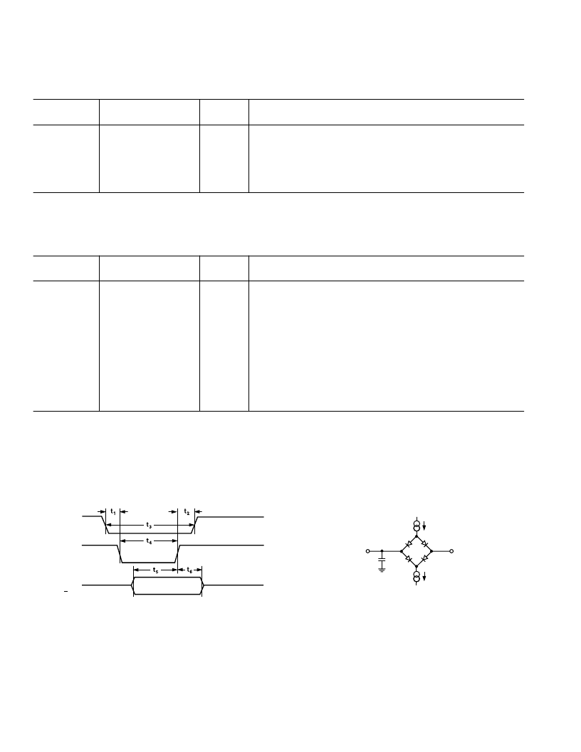
These numbers are measured with the load circuit of Figure 2.
Specifications subject to change without notice.
PARALLEL INTERFACE TIMING DIAGRAMS
CS
WR
A4
–
A0, CAL,
OFFS SEL
Figure 1. Parallel Write (SHA Mode Only)
I
OL
200 A
I
OH
200 A
C
50pF
TO
OUTPUT
PIN
1.6V
Figure 2. Load Circuit for D
OUT
Timing Specifications
发布紧急采购,3分钟左右您将得到回复。
相关PDF资料
EVAL-AD5533EB
32-Channel Precision Infinite Sample-and-Hold
Eval-AD5570EB
True Accuracy, 16-Bit 12 V/15 V, Serial Input Voltage Output DAC
EVAL-AD5620EB
Single, 12-/14-/16-Bit nanoDAC with 5 ppm/C On-Chip Reference in SOT-23
EVAL-AD5663REB
Dual 12-/14-/16-Bit nanoDAC with 5 ppm/C On-Chip Reference
EVAL-AD5664REB
Quad, 12-/14-/16-Bit nanoDACs with 5 ppm/C On-Chip Reference
EVAL-AD5666EB
Quad, 16-Bit DAC with 5 ppm/C On-Chip Reference in 14-Lead TSSOP
EVAL-AD5680EB
5 V 18-Bit nanoDAC in a SOT-23
EVAL-AD5821EBZ1
120 mA, Current Sinking, 10-Bit, I2C DAC
相关代理商/技术参数
EVAL-AD5532EBZ
功能描述:BOARD EVAL FOR AD5532 RoHS:是 类别:编程器,开发系统 >> 评估板 - 数模转换器 (DAC) 系列:- 产品培训模块:Lead (SnPb) Finish for COTS
Obsolescence Mitigation Program 标准包装:1 系列:- DAC 的数量:4 位数:12 采样率(每秒):- 数据接口:串行,SPI? 设置时间:3µs DAC 型:电流/电压 工作温度:-40°C ~ 85°C 已供物品:板 已用 IC / 零件:MAX5581
EVAL-AD5532HSEBZ
功能描述:BOARD EVAL FOR AD5532HS RoHS:是 类别:编程器,开发系统 >> 评估板 - 数模转换器 (DAC) 系列:- 产品培训模块:Lead (SnPb) Finish for COTS
Obsolescence Mitigation Program 标准包装:1 系列:- DAC 的数量:4 位数:12 采样率(每秒):- 数据接口:串行,SPI? 设置时间:3µs DAC 型:电流/电压 工作温度:-40°C ~ 85°C 已供物品:板 已用 IC / 零件:MAX5581
EVAL-AD5533EB
制造商:AD 制造商全称:Analog Devices 功能描述:32-Channel Precision Infinite Sample-and-Hold
EVAL-AD5535BEBZ
功能描述:数据转换 IC 开发工具
RoHS:否 制造商:Texas Instruments 产品:Demonstration Kits 类型:ADC 工具用于评估:ADS130E08 接口类型:SPI 工作电源电压:- 6 V to + 6 V
EVAL-AD5535EB
制造商:Analog Devices 功能描述:Evaluation Board For AD5535 制造商:Analog Devices 功能描述:EVALUATION BOARD I.C. - Bulk
EVAL-AD5535EBZ
功能描述:BOARD EVALUATION FOR AD5535 RoHS:是 类别:编程器,开发系统 >> 评估板 - 数模转换器 (DAC) 系列:- 产品培训模块:Lead (SnPb) Finish for COTS
Obsolescence Mitigation Program 标准包装:1 系列:- DAC 的数量:4 位数:12 采样率(每秒):- 数据接口:串行,SPI? 设置时间:3µs DAC 型:电流/电压 工作温度:-40°C ~ 85°C 已供物品:板 已用 IC / 零件:MAX5581
EVAL-AD5541/42EB
制造商:Analog Devices 功能描述:Evaluation Kit For AD5541 5 V, Serial-Input, Voltage-Output, 16-Bit DACs 制造商:Analog Devices 功能描述:EVALUATION BOARD I.C. - Bulk
EVAL-AD5541/42EBZ
功能描述:BOARD EVAL FOR AD5441/2 RoHS:是 类别:编程器,开发系统 >> 评估板 - 数模转换器 (DAC) 系列:- 产品培训模块:Lead (SnPb) Finish for COTS
Obsolescence Mitigation Program 标准包装:1 系列:- DAC 的数量:4 位数:12 采样率(每秒):- 数据接口:串行,SPI? 设置时间:3µs DAC 型:电流/电压 工作温度:-40°C ~ 85°C 已供物品:板 已用 IC / 零件:MAX5581